This content is reproduced with the kind permission of the original author Mike Brenner and was originally published at Stockopedia
Why Graphene?
It’s a multifunctional material that can be added to other materials to change their properties
- It is ultra-light yet immensely tough.
- It is 200 times stronger than steel, but it is incredibly flexible.
- It is the thinnest material possible as well as being transparent.
- It is a superb conductor and can act as a perfect barrier – not even helium can pass through it.
- In its graphene oxide form it is the worlds finest membrane – you can remove salts from water to create drinking water
What applications for graphene?
- http://www.graphene.manchester.ac.uk/explore/the-applications/
- http://www.techradar.com/news/20-ways-graphene-is-about-to-change-your-life
Some video’s on its background and uses:
- Graphene: Made in Manchester – https://www.youtube.com/watch?v=ZMJnBx117-E
- What is Graphene – https://www.youtube.com/watch?v=0fbQX5VJmew
- Energy – https://www.youtube.com/watch?v=DzLiaJsric4
- Composite Materials – https://www.youtube.com/watch?v=LTa_ileMJxE
- Membranes – https://www.youtube.com/watch?…
Further down I refer to many actual use cases / latest research but the easiest way to think about is that it these advanced materials which include graphene will profoundly change society and everything we see and touch.
Hang on if this stuff is so bloody amazing then what has been holding it back
Producing Graphene- Scale, Quality, Cost
The isolation of graphene at The University of Manchester led to the discovery of a whole family of 2D materials, including hexagonal boron nitride (sometime known as white graphene), molybdenum disulphide and phosphorene. Its estimated that there are two thousand 2D materials and many of them have not been researched so there are decades of future opportunities to be discoved. These 2D materials can be combined to create new ‘designer advanced materials’ to produce applications originally limited to science fiction.
Types of Graphene
There are many ways in which scientists are able to create or isolate graphene. Graphene can exist as tiny flakes, large sheets or in a solution.
- Complicated by the fact that there are many different types of Graphene and many target markets
- Graphene – A single-atom-thick sheet of hexagonally arranged, bonded carbon atoms, either freely suspended or adhered to a substrate. The dimensions of graphene can vary from several nanometers to the macroscale. Monolayer (single-layer) graphene is the purest from available and is useful for high-frequency electronics. Bi- and tri-layer graphene, two and three layers respectively, display a range of different qualities as the number of layers increase, as well as becoming progressively cheaper as the layers multiply.
- Few-layer graphene (FLG) or multi-layer graphene (MLG) – A 2D, sheet-like material, either as a free-standing flake or substrate-bound coating, consisting of a small number (between two and about 10) of well-defined, countable, stacked graphene layers of extended lateral dimension. Individual flakes should still maintain a high aspect ratio. Few-layer graphene or graphene oxide dispersions can have a defined thickness distribution. MLG is useful for composite materials, and as a mechanical reinforcement.
- Graphene oxide (GO) – Chemically modified graphene prepared by oxidation and exfoliation. Graphene oxide is a monolayer material with a high oxygen content. Thin membranes that allow water to pass through but block off harmful gases are a major use for GO.
- Reduced graphene oxide (rGO) – Graphene oxide (as above) that has been reductively processed by chemical, thermal, microwave, photo-chemical, photo-thermal or microbial/bacterial methods to reduce its oxygen content. Conductive inks are just one potential use for rGO.
- Each type of “Graphene” offers a different set of properties depending on the form in which it arrives.
- Similarly, each target market also requires different performance levels and cost targets.
My Opinion – What really matters is a) can you produce graphene that meets the ISO standards so that its got the properties of graphene b) can you produce it in a commercially viable way (quantity, quality, price and end applications able to use it and end customers). As you will see later on, Few Layer graphene and Reduced Graphene Oxide are the two key types that can answer yes to both questions
Different Processes to Produce Graphene
Many research institutions around the world are currently racing to find the best, most efficient and effective way of producing high quality graphene on a large scale, which is also cost efficient and scalable. Below are 4 main methods (note there are more out there in theory, not necessarily in practise!):
- Chemical vapour deposition (CVD) – CVD extracts carbon atoms from a carbon rich source (typically a gas) by reduction and deposits gaseous reactants onto a heated substrate such as silicon, nickel or copper. Gas molecules are combined in a reaction chamber, the resulting reaction creates a graphene film upon contact with the substrate. The benefits of using CVD to deposit materials onto a substrate are that the quality of the resulting materials is usually very high – as a result it’s the most common way for scientists to create monolayer or few layer graphene.
My Opinion: For IQE fans, this is basically what they do to create their advance semi-conductor wafer products but with different materials. The main problem with this method is finding the most suitable substrate to grow graphene layers on, and developing an effective way of removing the graphene layers from the substrate without damaging or modifying the atomic structure of the graphene. Ultimately it is still to be proven if it is commercially viable in being able to produce enough graphene, of a high enough quality and a suitable price. There will always be applications (esp mid to long term medical, replacing silicon chips), but this is currently holding back many graphene producing companies from scaling out of the lab into creating graphene enhanced products with partners which is why most companies operating this process are money pits
- Mechanical exfoliation of graphene – Mechanical exfoliation is the original method used by Prof Sir Andre Geim and Prof Sir Kostya Novoselov to isolate a single graphene flake. Scotch tape was used to remove layers from bulk graphite, these layers are then transferred to a substrate such as silicon. On removing the tape single layer graphene with large crystal sizes is left on the substrate.
My Opinion: exfoliation produces graphene with the lowest number of defects and highest electron mobility – 3M would be keen if we used Scotch Tap still, however this is the process that the University of Manchester focussed on with their 2D-Tech Graphene production company in partnership with the University of Ulster who patented the process to create high quality few layers of Graphene – this process is also sometimes called grinding. http://www.2-dtech.com were acquired by Versarien in 2014 from the University of Manchester, and Versarien then secured an exclusive global license with the University of Ulster for their patented exfoliation process to create Nanene https://www.nanene.com … a lot more on this later!
- Liquid exfoliation of graphene – Liquid exfoliation of graphite typically involves blasting the raw bulk material into small fragments of graphene using ultrasonic energy. Powdered graphite is typically sonicated in a solvent over a number of hours to extract individual layers.
My Opinion: To keep good lateral sizes, many methods smash them all to bits giving a limited lateral size average. Edges of plates get damaged, cracks and holes can be created all which weaken the Graphene nanoplatelets (GNPs), they can crumple and fold. You must have a manufacturing process that is both severe enough to get the layer level but gentle enough to limit the damage and maintain lateral sizes. Many of the manufacturers struggle to get usable graphene flakes of a high enough quality with their blasting so end up creating a “thin graphite solution” (See competitors section). A new method for producing high quality conductive graphene inks with high concentrations has been developed in a collaboration led by researchers working at the Cambridge Graphene Centre at the University of Cambridge, UK. The novel method uses ultrahigh shear forces in a microfluidisation process to exfoliate graphene flakes from graphite. The process converts 100% of the starting graphite material into usable flakes for conductive inks, avoiding the need for centrifugation and reducing the time taken to produce a usable ink. Inks produced using this method have already been patented and commercialised via a University of Cambridge spin out company, Cambridge Graphene http://www.cambridgegraphene.com , which was recently acquired by engineering solutions company Versarien in Jan 2017 … much more on this later!
- Electrochemical exfoliation of graphene (Sometimes called Graphite Oxide Reduction) – Electrochemical exfoliation is one phase of liquid exfoliation. An electrode of graphite is introduced to a solvent with a current applied. If the graphite is positive electrode graphene oxide is produced, conversely when the graphite is present at the negative electrode non-oxidised graphene flakes are produced. The graphene or graphene oxide will deposit at the bottom of the reaction chamber.
My Opinion: This latter method of using heat (either by atomic force microscope or laser) to reduce graphite oxide to graphene has received a lot of publicity of late due to the minimal cost of production. However, the quality of graphene produced currently falls short of theoretical potential and will inevitably take some time to perfect. New ISO standards will sort the wheat from the chaf (See competitors section on graphite producers producing “tonnes of graphene”!)
Standards
Graphene has not had standards so it’s difficult for customers to be assured of the quality and properties of its graphene samples and of the applications and products they wish to enhance and create.
- Investors & big companies are sick to death of dozens of small graphene companies saying, “we have fantastic graphene”, none of which ever seems to work.
- See competitor section for lost of insights on this pain!
Material standardisation is key to accelerate the development of graphene-enabled technology and improve the ability to produce graphene in a reliable and repeatable way.
- A nice presentation going into the standards for graphene – www.rsc.org/events/download/Document/1ebfc5bf-48ca-48e4-a6be-9065bccb508c
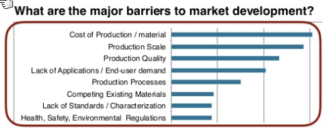
Market challenges:
1. Slow pace of standards development
The University of Manchester and the National Physical Laboratory (NPL) partnered in 2013 to work together on the development of graphene standards, metrology and characterisation so they could answer 2 key questions:
- What are the characteristics of the produced material?
- How it can be used and tested to prove its graphene enhanced’?
- First ISO Graphene Standards launched in October 2017: The new international standard, led by the National Physical Laboratory (NPL), defines the terminology used to describe the many different forms of graphene and related 2D materials, supporting companies in the testing and validation of the ‘wonder material’. This will provide clarity among manufacturers, suppliers, NGOs and academia, helping to unlock new applications, drive down manufacturing costs and open up the industrial-scale use of graphene for applications from next-generation computer chips to smart sensors in clothing. After a rigorous development process involving technical experts from 37 different countries, the standard is now available online and contains 99 terms and definitions covering the types of 2D materials, material production, material characterisation and material properties. http://www.npl.co.uk/news/first-graphene-iso-standard-published-to-boost-commercialisation
- Characterisation is the measurement of the properties of the material – You need to be able to detect, identify & characterise graphene in various types, sizes, shapes and chemical functionality. Nice video explaining: https://phys.org/news/2017-11-characterisation-graphene.html
- The new guidelines show how complex it is to answer the questions “is this graphene?” http://www.npl.co.uk/upload/pdf/gpg145_graphene.pdf
- Many other international and national bodies are looking at replicating these standards to enable their graphene industries to flourish as today without them they are floundering. E.g. China (see interesting development on proposed JV with Versarien for Nanene in manufacturing section) https://www.google.co.uk/amp/m.scmp.com/tech/innovation/article/2114455/soaring-share-prices-chinese-graphene-companies-prompts-bubble%3famp=1
2. Application of the word graphene to materials many different forms of carbon
· Prior to the publication of the ISO standard, as there were no universally-agreed definitions. NPL’s Dr Andrew Pollard, who co-led the development of the standard with Dr Charles Clifford, commented: “Both graphene producers and end-users have been concerned for years that inconsistent terminology has meant slower progress in the commercialisation of these materials and made it difficult to determine the difference between graphene and graphite products. Although it may be understood that the term ‘graphene’ means a single layer of graphene, the vagueness of terms such as ‘few-layer graphene’ has blurred the line between graphene and graphite. This terminology standard addresses this barrier and is the first step in standardisation of this emerging industry.” http://www.npl.co.uk/news/first-graphene-iso-standard-published-to-boost-commercialisation
- Graphene Vs Graphite – Graphene is fundamentally one single layer of graphite, but it offers some impressive properties that exceed those of graphite as it is isolated from its ‘mother material’.
- Strength – Graphite is naturally a very brittle compound and cannot be used as a structural material on its own due to its sheer planes (although it is often used to reinforce steel).
- Graphene, on the other hand, is the strongest material ever recorded.
- Electrical properties – Due to graphite’s planar structure, its thermal, acoustic and electronic properties are highly dependent on the direction of travel of phonons e.g. they travel much more easily along the planes than they do when attempting to travel through the planes.
- Graphene, on the other hand, being a single layer of atoms and having very high electron mobility, offers fantastic levels of electronic conduction due to the occurrence of a free pi (π) electron for each carbon atom.
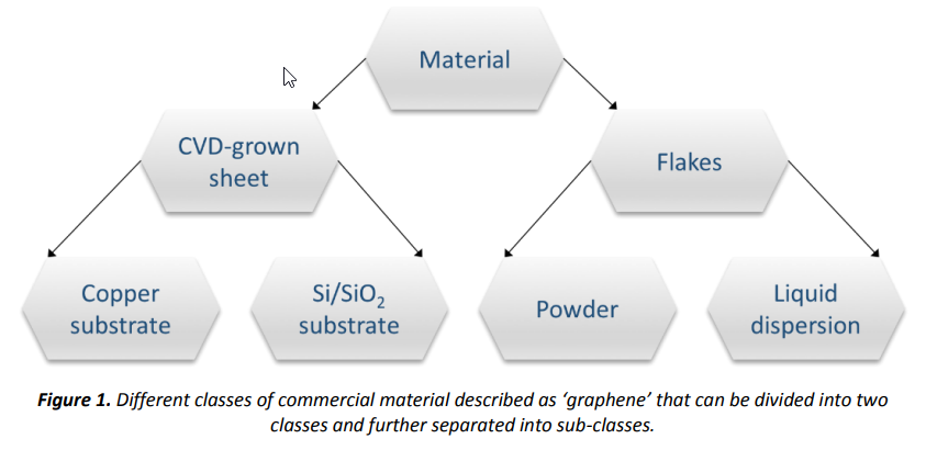
- the substrate coverage of a CVD-grown graphene sheet e.g. Copper or Silicon
- the number of layers/thickness of the graphene – under 10 layers meet the ISO
- powder or liquid dispersions that contain graphene flakes typically also contain flakes of different thicknesses and lateral sizes, depending on the process conditions used e.g. mechanical exfoliation from graphite, or other processes.
- the lateral dimensions of flakes
- layer alignment
- the level of disorder
There are very few graphene producers who publish reports of independent experts with independent data on tests of their graphene that meet any international standards. Most are “paid for research” and not from credible Universities with a skill set or the right testing machines, so this is a red flag to look for in any graphene producers / competitors.
4. Inconsistency in the production of materials and lack of material verification to assure buyers of quality and performance characteristics
- Standards and testing needs to be developed on the structural and chemical characterisation and electrical properties of graphene not just in its produced form, but also to test it within the applications its applied to e.g. plastic composites, carbon fibre, electronic devices, batteries etc …
o http://www.npl.co.uk/topics/graphene/structural-analysis-of-graphene-and-related-2d-materials/
§ The key is to advance graphene research and standards to be able to test and optimise the impact of graphene on applications e.g. allergen detection in food manufacturing and prove to customers that a) the product used was ISO standard graphene b) their specific application is inheriting the capabilities of graphene c) the manufacturing process end to end when scaled up will enable this
Patents
You cannot patent graphene as it’s a naturally occurring material – carbon. Many organisations however, have patented graphene devices and manufacturing processes. The UK is often criticised for falling behind competitors in terms of number of patents filed. There are many thousands of patents relating to graphene but many of these may are unlikely to become reality.
The University of Manchester believes academic partnership with industry and a collaborative approach to research and development is a more logical approach to exploit graphene’s superlative properties and realise its commercial prospects. Patenting isn’t just a numbers game it’s about quality not quantity.
“Innovation is about much more than patents. As a rule of thumb, one should apply for a patent only if there is a clear route to a commercial product. Even then, there are many ways to fail – but at least the patent will not serve as an expensive memorial to your vanity.” Prof Sir Andre Geim
My Opinion – Key problems with patents are the speed that they are granted, and that once submitted you help your competitors understand how things work. Often this leads to long and expensive battles in court arguing about if IP has been copied, which in many cases slows companies down and stops them achieving their potential. Sometimes you are better off innovating faster, using patents only in key places and instead relying on keeping things secret to the outside world. After all it works well for Coca Cola!
See section in Part 2 on VRS, patents and protecting IP
Graphene Research in the UK
Research Gateway is an amazing resource where you can see specific project funding and amounts, by which organisations (e.g. innovate UK, graphene flagship, industry collaborators) and the outcomes of research. Gives an idea of how what has been done in the past and what applications are being researched now.
For example
- Search for all Graphene funded research in the UK – http://gtr.rcuk.ac.uk/search/project?term=graphene&fetchSize=25&selectedSortableField=&selectedSortOrder=&fields=acp.d%2Cis.t%2Cprod.t%2Cpol.oid%2Cacp.oid%2Crtp.t%2Cpol.in%2Cprod.i%2Cper.pro.abs%2Cacp.i%2Ccol.org%2Cacp.t%2Cis.d%2Cis.oid%2Ccpro.rtpc%2Cprod.d%2Cstp.oid%2Crtp.i%2Crdm.oid%2Crtp.d%2Ccol.dept%2Cff.d%2Cff.c%2Ccol.pc%2Cpub.t%2Ckf.d%2Cdis.t%2Ccol.oid%2Cpro.t%2Cper.sn%2Corg.orcidId%2Cper.on%2Cff.dept%2Crdm.t%2Corg.n%2Cdis.d%2Cprod.oid%2Cso.cn%2Cdis.i%2Cpro.a%2Cpub.orcidId%2Cpol.gt%2Crdm.i%2Crdm.d%2Cso.oid%2Cper.fnsn%2Cper.org.n%2Cper.pro.t%2Cpro.orcidId%2Cpub.a%2Ccol.d%2Cper.orcidId%2Ccol.c%2Cip.i%2Cpro.gr%2Cpol.i%2Cso.t%2Cper.fn%2Ccol.i%2Cip.t%2Cff.oid%2Cstp.i%2Cso.i%2Ccpro.rcpgm%2Ccpro.hlt%2Ccol.pic%2Cso.d%2Cff.t%2Cip.d%2Cdis.oid%2Cip.oid%2Cstp.d%2Crtp.oid%2Cff.org%2Ckf.oid%2Cstp.t&type=
- Specific project – Graphene Flexible Electronics and Optoelectronics project at the university of Cambridge shows http://gtr.rcuk.ac.uk/projects?ref=EP%2FK01711X%2F1
- If you search on the key people you can see all of the research they do into graphene, but most interestingly for us which companies and universities they collaborate with e.g.
- Professor Andrea Ferrari – http://gtr.rcuk.ac.uk/person/CF1565B8-F3ED-4269-9207-ED06C96373B8
- Kostas Kostarelos from the University of Manchester – http://gtr.rcuk.ac.uk/person/42128CD3-748A-4599-A4FA-AEF2F31A5835
- National Graphene Institute – you can see all collaborations and research published so far – http://gtr.rcuk.ac.uk/projects?ref=EP%2FK005014%2F1
My Opinion – Versarien have received lots of funding through the Innovate UK – If you download the excel you can see all the past, current and future projects that Versarien, 2D-Tech and Cambridge Graphene Ltd are working on – https://www.gov.uk/government/publications/innovate-uk-funded-projects